Build Guide¶
1. 3D Printing Guidelines¶
Parts are designed and oriented optimally for fused deposition modeling (FDM) 3D printing. Parts pictured in proceeding sections were printed on a Prusa i3 MK3S 3D printer in “Galaxy Black” or “Azure Blue” Prusament PLA.
If a 3D printer is not available there are many 3D printing services available, e.g. ShapeWays in the US, or Xometry in the EU, that will ship parts directly to you and offer online quotes after uploading the STLs. If ordering through a service, it’s recommended to order as many of the consumable skimmer clamps as possible to avoid re-ordering later on.
- For 3D printing services we recommend:
Type/technology: FDM/FFF
Material: PLA
Layer height (sometimes called resolution): 0.1-0.2 mm
No support material
FETbox Enclosure¶
Depending on several printer-specific conditions including parting cooling, print speed, and material properties, it may be necessary to clean up the overhangs and bridge areas:
Areas that may require post-print clean-up to remove hanging material.¶
Skimmer Clamp¶
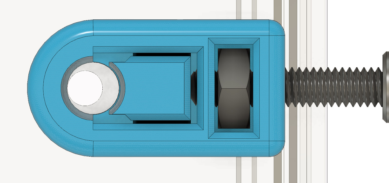
This part was modelled with a print-in-place sliding mechanism for securely clamping the P200 tip in place without potentially damaging it with bolt.
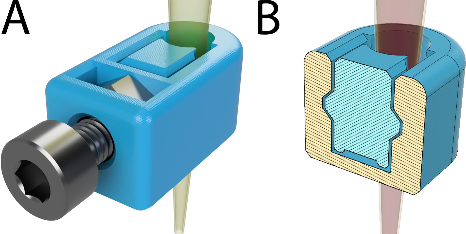
A) Skimmer clamp, assembled. B) Print-in-place clamping mechanism. Note how the slide does not contact the surrounding clamp body at any point but is fully contained.¶
The clamp slide should break free with minimal effort and then slide freely after using the method described here. Because of the small size of this part, printing just one at a time can lead to overheating artifacts. Print at least two or three at once while optimizing print settings.
Tip
Most popular slicing software have the option to reduce the material flowrate on un-supported extrusions. The first layers of the underside of the clamp benefit from this feature.
Using PrusaSlicer 2.2.0 [1] we had success with a bridge flow ratio of 0.7, for example.
Tip
It may also be advantageous to use a 0.1 mm layer height for this part as less material is deposited at once and is less likely to adhere irreversibly unintended layers below.
Skimmer Nozzle Height Blocks¶
The thickness of the nozzle height setting blocks (and consequently the skimmer nozzle height) is particularly sensitive to first layer height calibration and it is recommended that the printed height be validated with a micrometer, high quality calipers, or more empirically by measuring the residual plate volume.
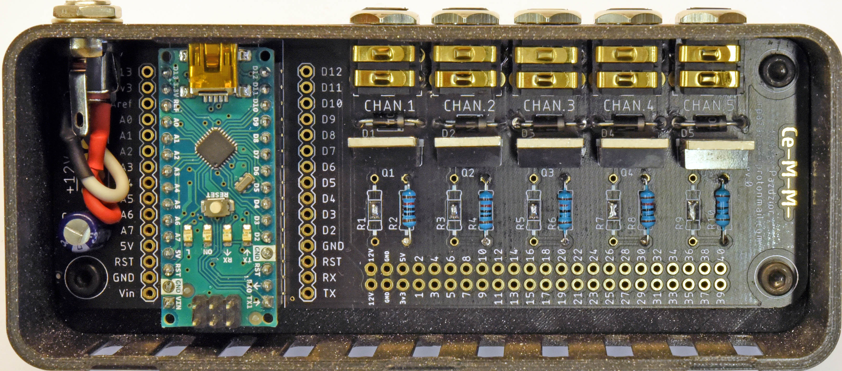
1. FETbox Hardware Controller¶
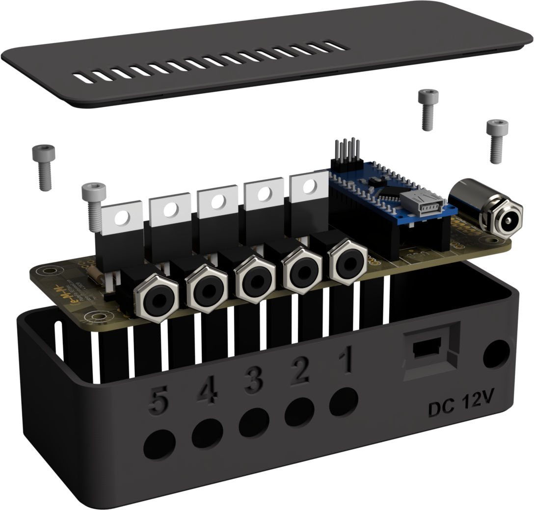
Exploded FETbox hardware controller.¶
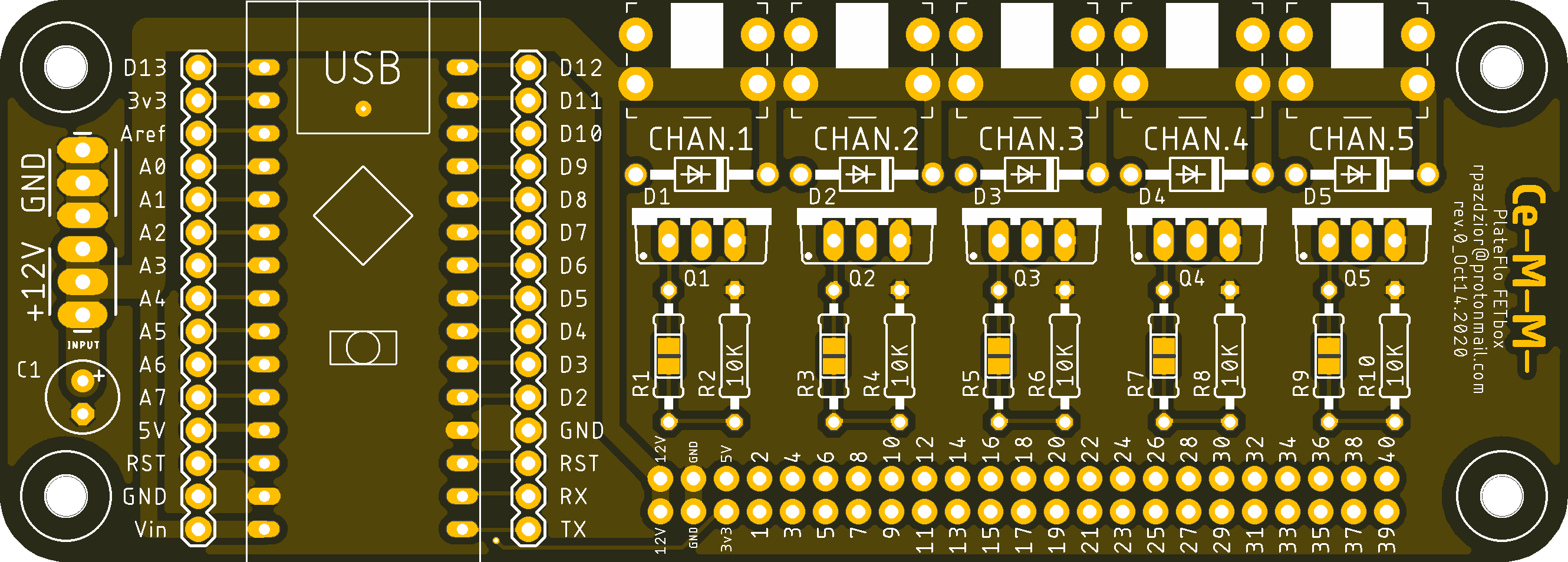
PCB Ordering¶
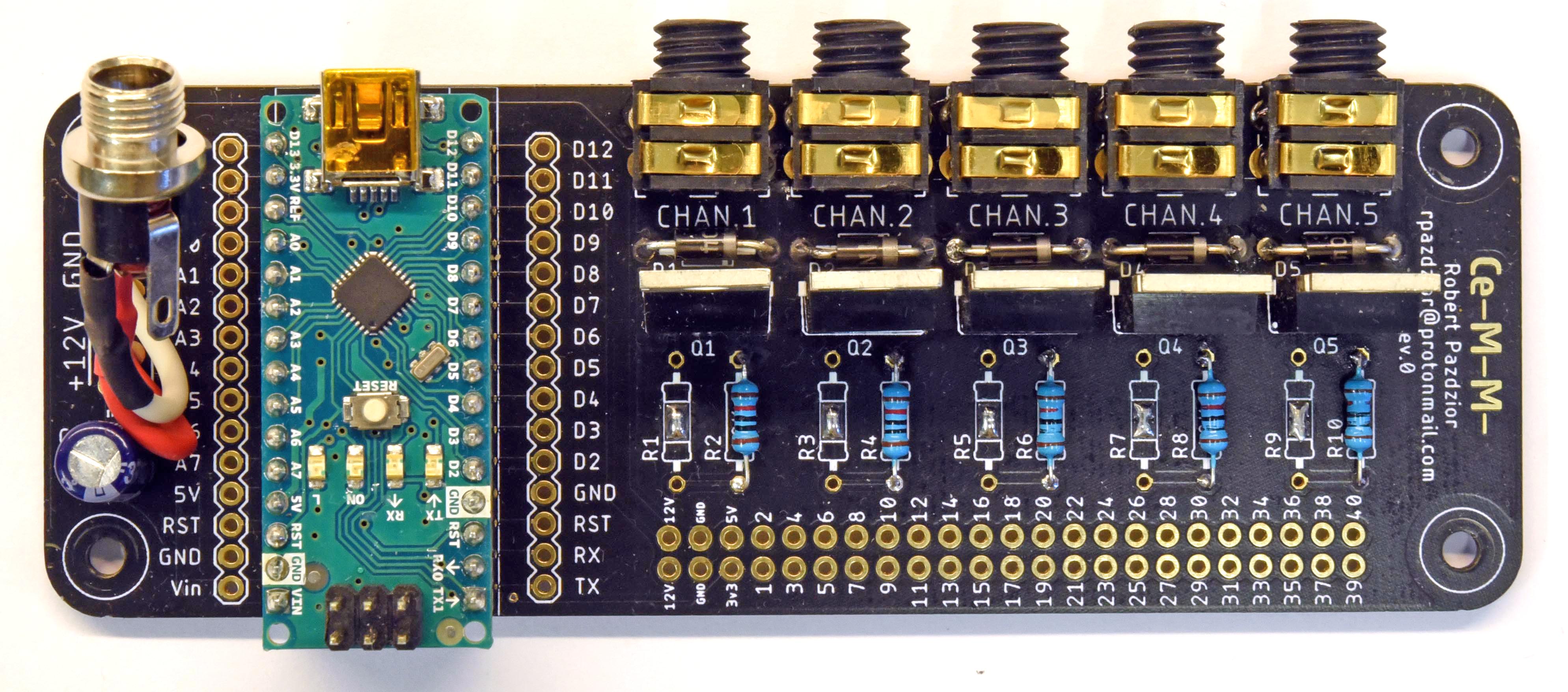
FETbox PCB render (top).¶
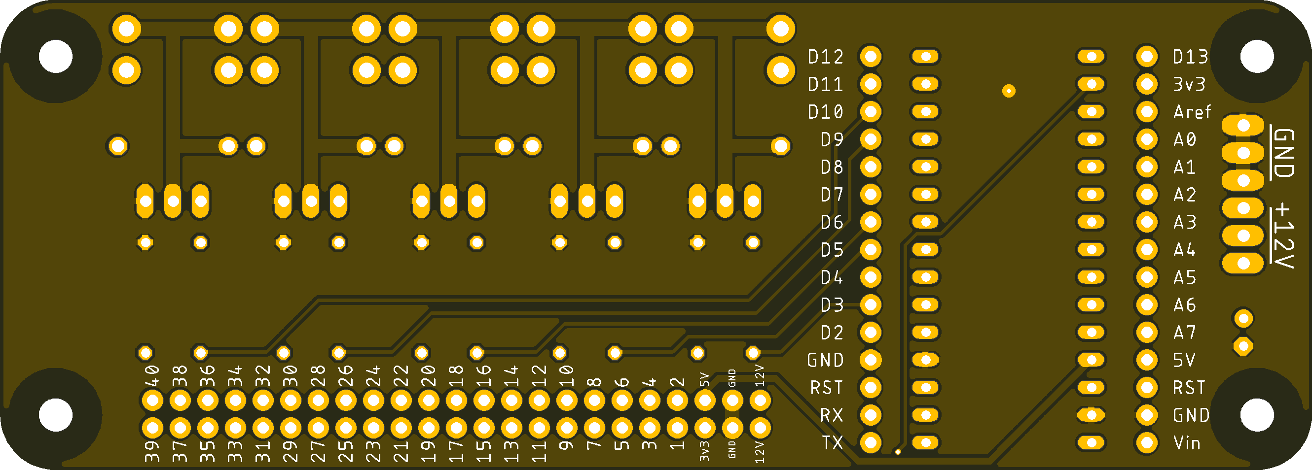
FETbox PCB render (bottom).¶
The FETbox printed circuit board (PCB) was designed with professional manufacture in mind and is not necessarily optimized for e.g. DIY milling/etching. There are many services available for small-run prototype PCB production, making it feasible to order several bare PCBs at an affordable rate.
At the time of writing, JLCPCB (China) [2] offers such a service and provided
the boards pictured herein. We opted for a black PCB and ENIG-RoHS surface
finish; however, these are optional and primarily cosmetic features in this
case. The included Gerber computer aided manufacturing (CAM) files were
generated according to JLCPCB’s capabilities [3] via Autodesk EAGLE [4] using
oxullo’s helper files [5], [6]. Similarly, FETbox_rev0_PCB.brd can be used
to generate CAM files for other PCB manufacturers using appropriate
specifications and EAGLE design software.
To place an order with JLCPCB, upload
FETbox_rev0_Gerber_JLCPCB.zip and select the PCB colour and surface finish
as desired. The board dimensions will be derived automatically from the Gerber
files.
Other options can be left in their default state:
2 layers
1 design
single PCB delivery format
1.6mm thickness
1 oz copper weight
no gold fingers, no production file confirmation
fully tested flying probe
no castellated holes
no order number removal.
PCB Assembly¶
Tip
For ease of assembly, it is recommended to solder diodes and resistors to the PCB prior to the output jacks and MOSFETS as the shorter components are more difficult to access once the taller MOSFETs and output jacks are mounted.
Tip
Axial component leads need to be bent 90° prior to soldering, this can be done with any pair of plyers, however a 3D-printed jig such as https://www.thingiverse.com/thing:26025 can make the task less finicky. Hole spacing on all diodes and resistors on the PCB are 0.4”/10.16 mm.
Instructions¶
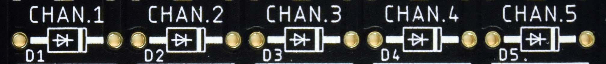
Solder the fly-back diodes (D1-D5) to the board. Ensure the polarity (white stripe) matches that on the PCB silkscreen.
Solder the 10kΩ pull-down resistors (R2, R4, R6, R8, R10) to the board.
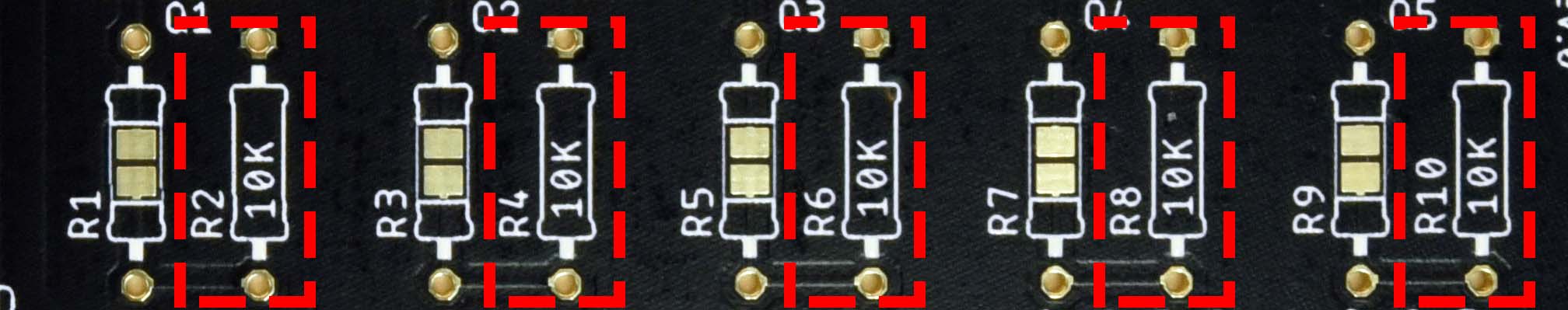
Optional: Current-limiting gate resistors can be added in the odd-numbered resistor positions (R1, R3, R5, etc.). Though they are not absolutely necessary in the author’s opinion.
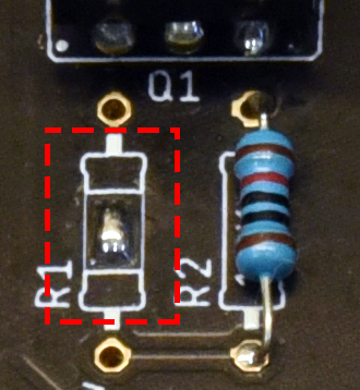
Caution
If a gate resistor is not used, the central pads at these positions must be bridged with solder as below.
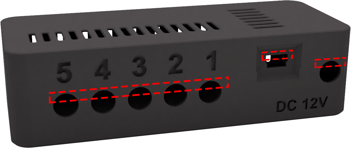
Solder the 3.5mm output jacks to the PCB. Note that due to the mass of copper around these solder pads conducting heat away, it may be necessary to increase the soldering iron temperature to make a proper joint here.
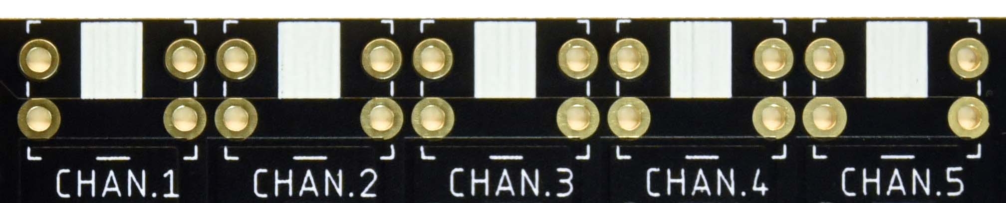
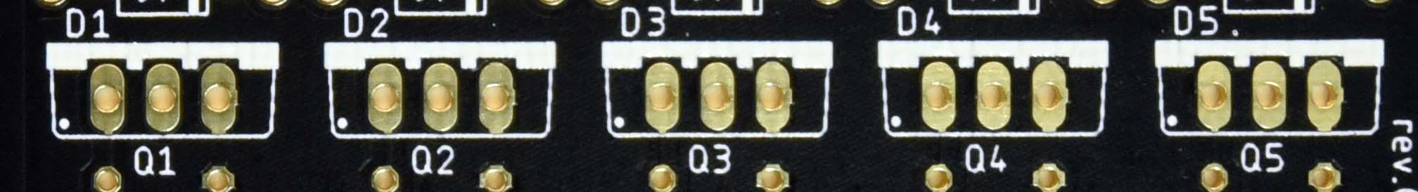
Solder the MOSFETs (Q1-Q5) to the PCB. As in the previous step, some of the MOSFETs pads will require more heat to make a proper joint here.
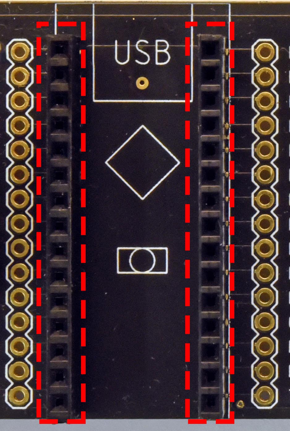
Trim two 30-pin strips from the female headers using side cutters.
Socket the Arduino Nano pins into the trimmed header strips before soldering the female headers to the board. This will ensure proper alignment and is easier to solder.
Solder the decoupling capacitor (C1) to the power input of board.
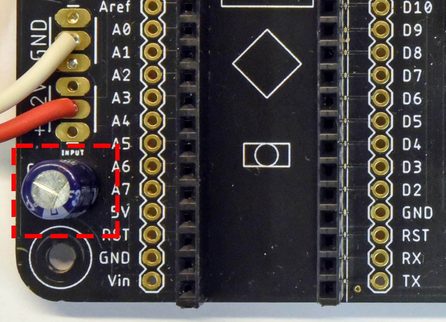
Warning
Take care with the polarity of the capacitor! The negative terminal will usually have a white stripe and/or shorter lead.
Reversing the polarity may cause the capacitor to explode.
Cut 2× 2-3 cm of 0.5mm2 (20 AWG) wire for the 12V DC input jack and strip a few millimeters from each end.
Solder one end of each wire to the barrel and center pin tabs of the DC jack, apply heat shrink tubing to the tabs if available.
Solder the DC jack center pin wire to one of the +12V solder pads at the power input. Likewise, for the barrel wire to one of the GND pads.
Tip
Additional pads, connected in parallel, are provided in case one wishes to power additional devices from the board input.
Bend the wires into a gentle loop away from the top edge of the board.
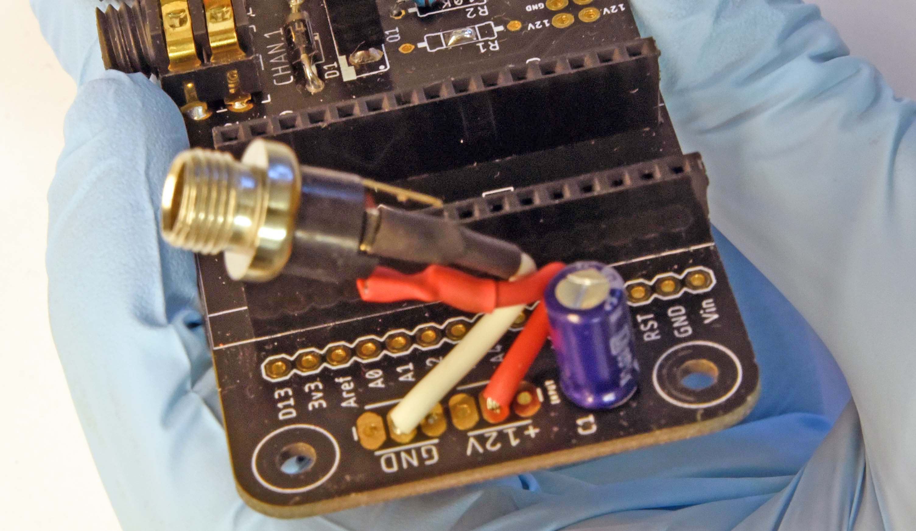
DC jack wired and soldered.¶
Trim excess leads from the bottom of the board using the side cutters if you have not done so already.
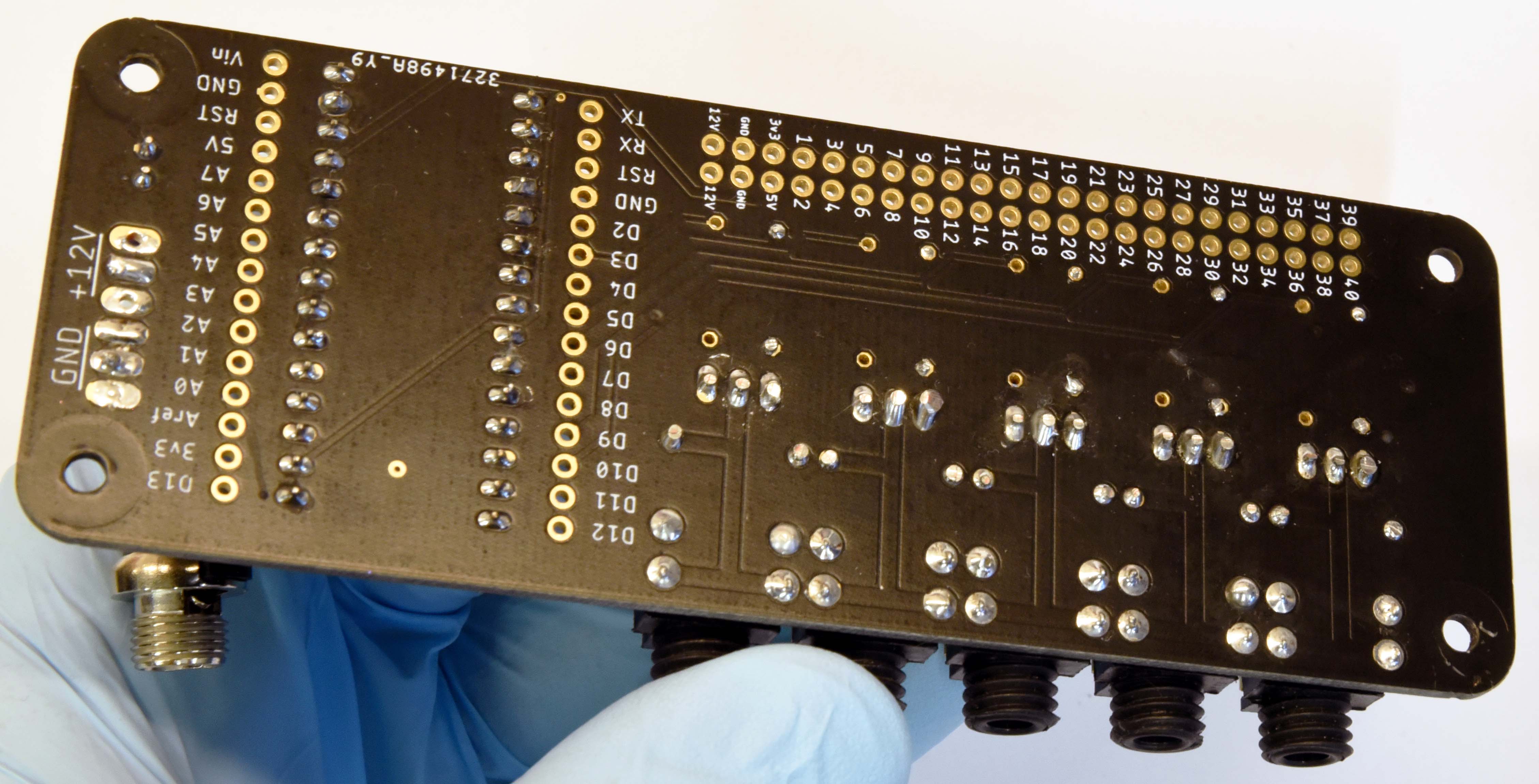
Soldered and trimmed leads.¶
Final Assembly¶
Using an M3×8 bolt, thread all four standoffs on the inside of the bottom half of the enclosure by driving the bolt in then out, one at a time. There will be significant resistance as the bolt cuts a thread into the printed plastic.
Warning
Do not overtighten! Plastic threads can be easily stripped.
Ensure there is adequate clearance for the M3 bolt to pass through the PCB mounting holes of the PCB.
PCB machining tolerance varies with manufacturer and a quick pass with a 3 mm drill bit or with the M3 bolt itself might be necessary.
Remove all nuts and washers from the DC jack and controller output jacks.
Socket the Arduino Nano into the controller board with its USB port oriented as printed on the PCB silkscreen.
Insert the board at an angle into the mounting holes of the enclosure. The board will sit flat with the base of the enclosure once these are through.
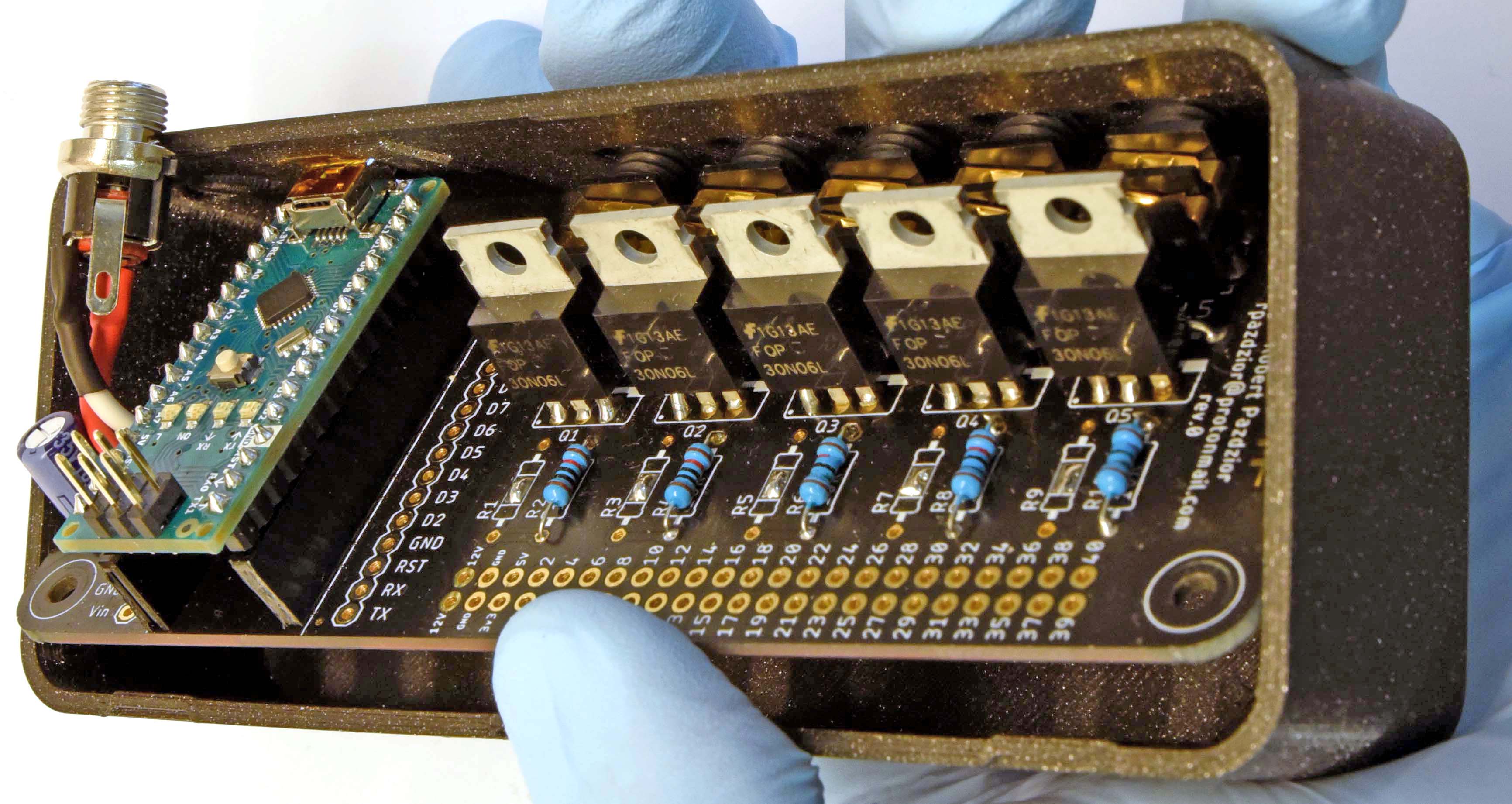
Secure the PCB to the enclosure bottom using four M3×8 bolts.
Re-install the washers and nuts for the DC input jack and controller output jacks. Do not overtighten the nuts on the output jacks.
Snap the enclosure lid in place with the convective cooling slots over the MOSFET array and Arduino.
Firmware Upload¶
The FETbox controller firmware is supplied as an Arduino ‘sketch’ for upload via the Arduino IDE software.
Install the Arduino IDE software and USB drivers per the instructions for your system.
Connect the hardware controller using a USB mini-B cable.
Open the hardware controller sketch, Firmware_FETbox.ino, with Arduino IDE.
Set the target board, processor and serial port:
Tools -> Board -> Arduino Nano,
Tools -> Processor -> ATmega328P,
Tools -> Port -> <Port>
Note: Tools -> Get Board Info can sometimes set these automatically.
Upload the sketch to the hardware controller Arduino:
Sketch -> Upload
Once uploaded, verify that the upload was successful:
Open the serial monitor: Tools -> Serial Monitor
Set the line ending to
Newlineand the baud rate to115200.Type
@#into the serial monitor and press Send or hit the Return key.
If the sketch was successfully uploaded, the board will respond with fetbox0
in the serial monitor.
3. Perfusion Plate¶
Skimmer Nozzle Clamp¶
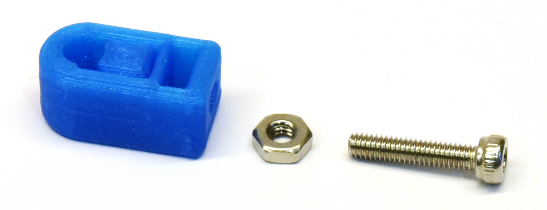
Parts, from left to right: printed skimmer_clamp_M3.stl,
M3 hex nut, M3 bolt.¶
Insert the M3 hex nut and thread in the M3 bolt until finger tight.
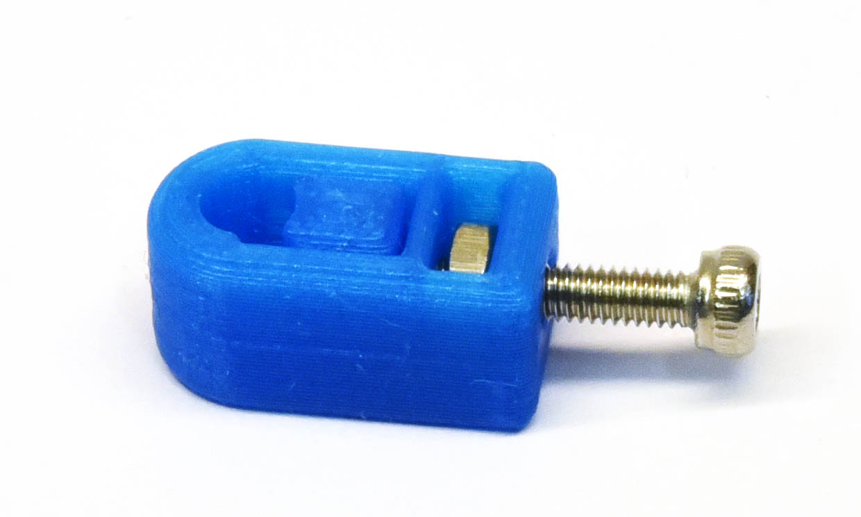
Using a 2.5 mm hex wrench, tighten sharply until the slide breaks free, then continue until the clamp slide has moved through its entire range of motion (below, right).
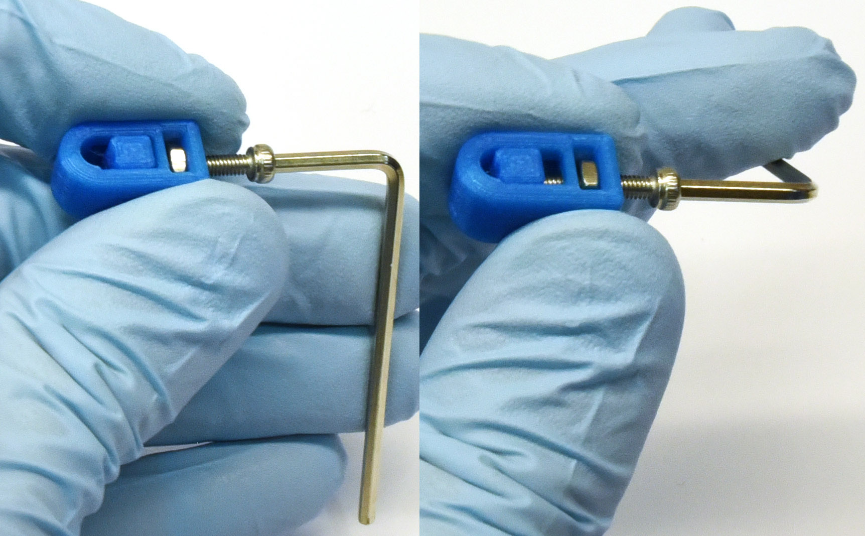
Left: Twist sharply to break the weak connection on the slide underside. Right Continue until the end of the slide travel range.¶
Back off the bolt until it is clear of the slide travel.
Using a small flat screwdriver or a P200 tip, push the slide back to its starting position.
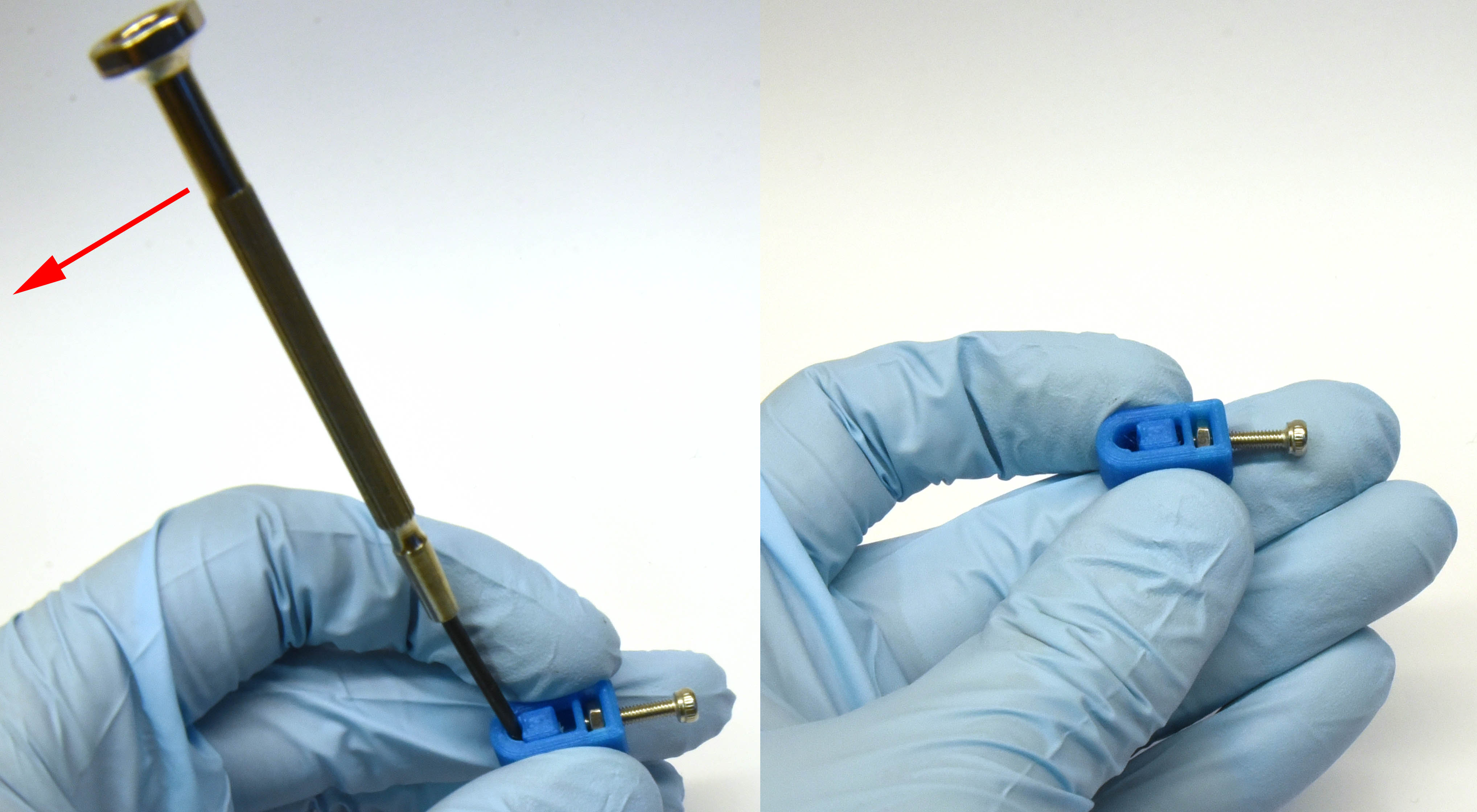
Left: use the screwdriver as a lever to push the slide back, there may be resistance the first time the slide moves. Right: The slide back in its starting position, ready for use.¶
Perfusion Plate Lid¶
See Petri Dish Perfusion Lid for notes on building the perfusion plate using a petri dish, rather than the recommended OmniTray.
Using the
perfusion_lid_drill_jigand a fine-tipped marker, transfer the four nozzle hole locations to the Nunc OmniTray lid.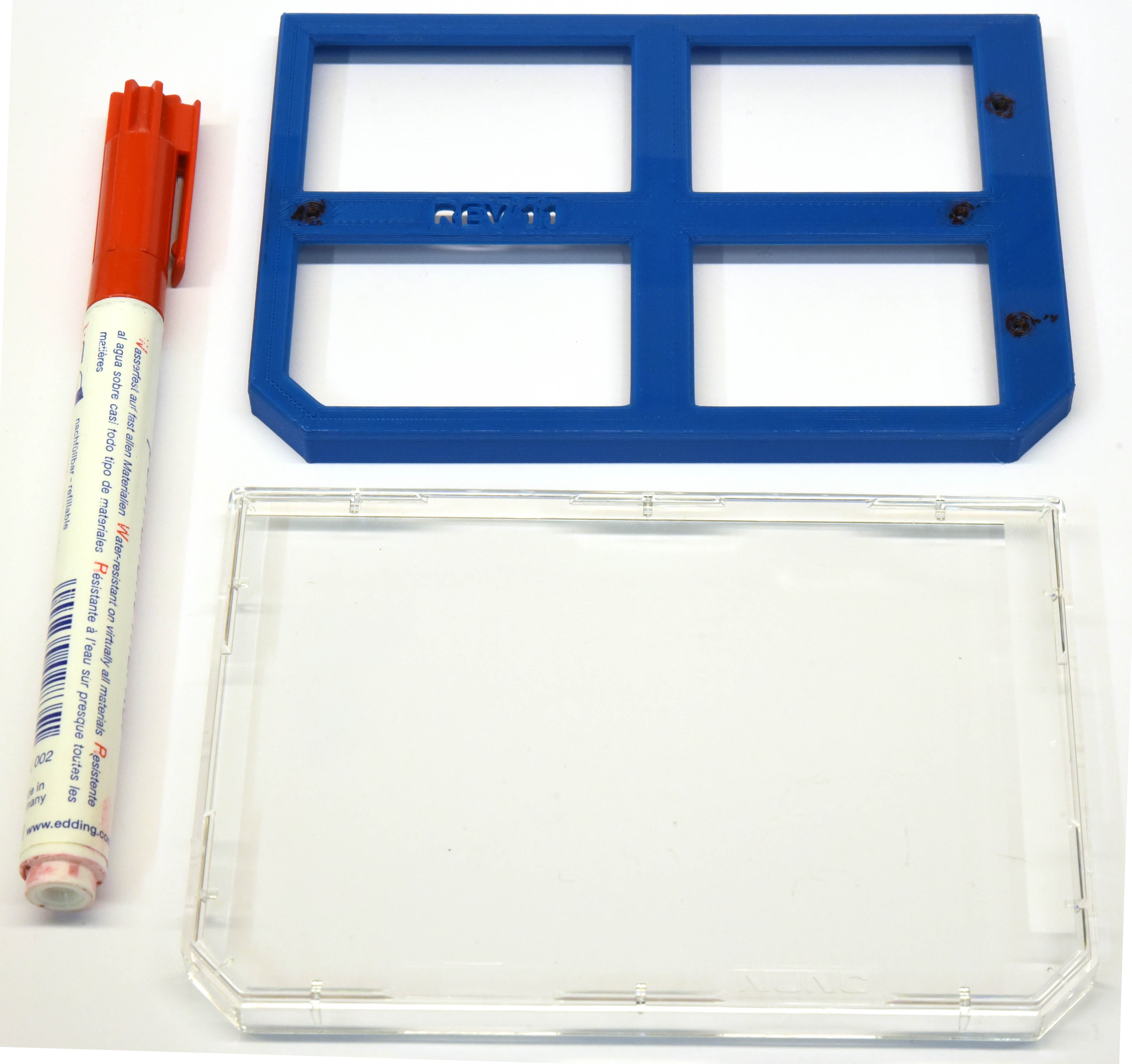
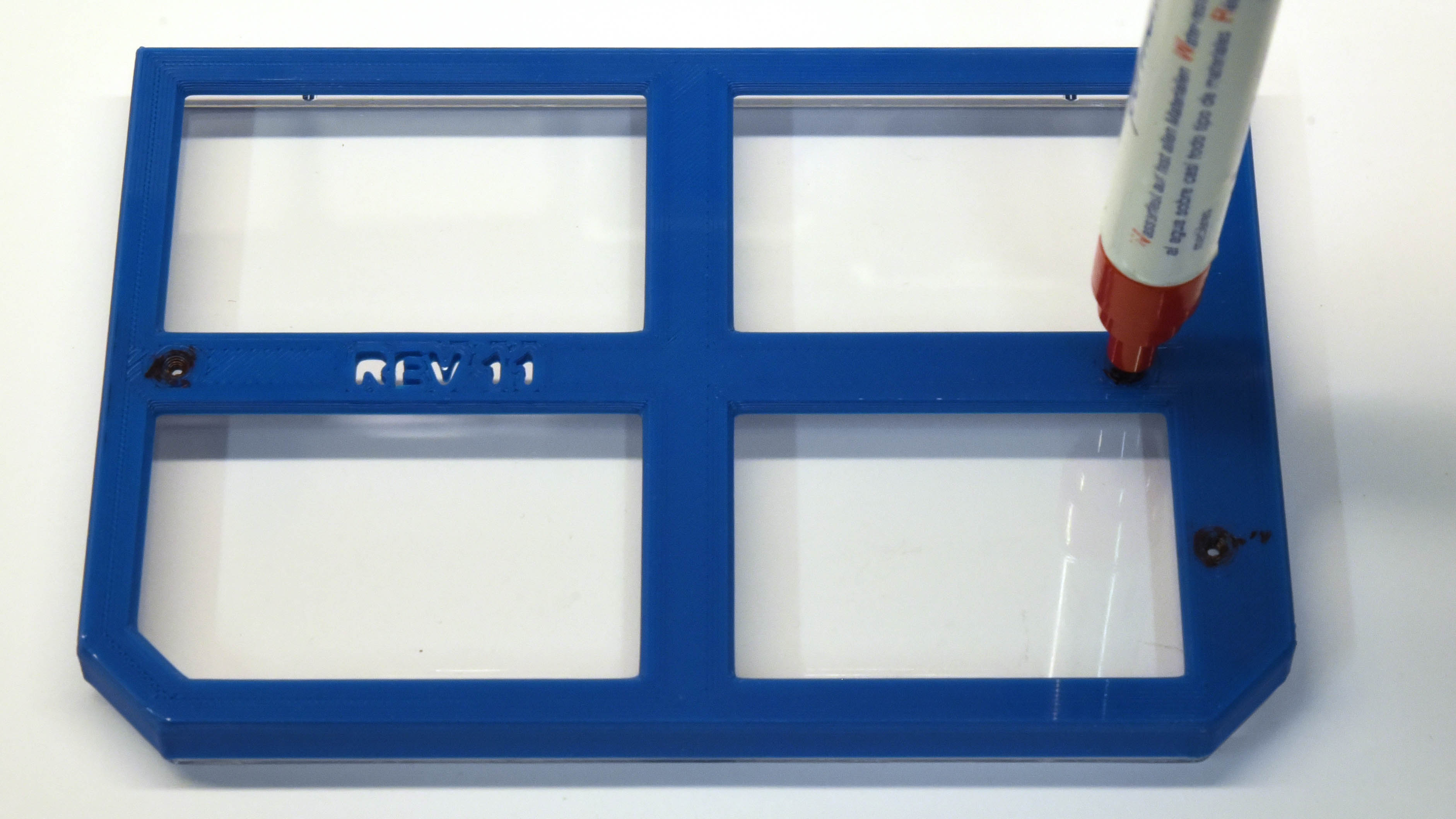
Using a 2.2mm[*] PCB milling bit/tool, drill all four marked holes.
Tip
Use a peck drilling technique to limit plastic melt and improve hole dimensional accuracy and consistency.
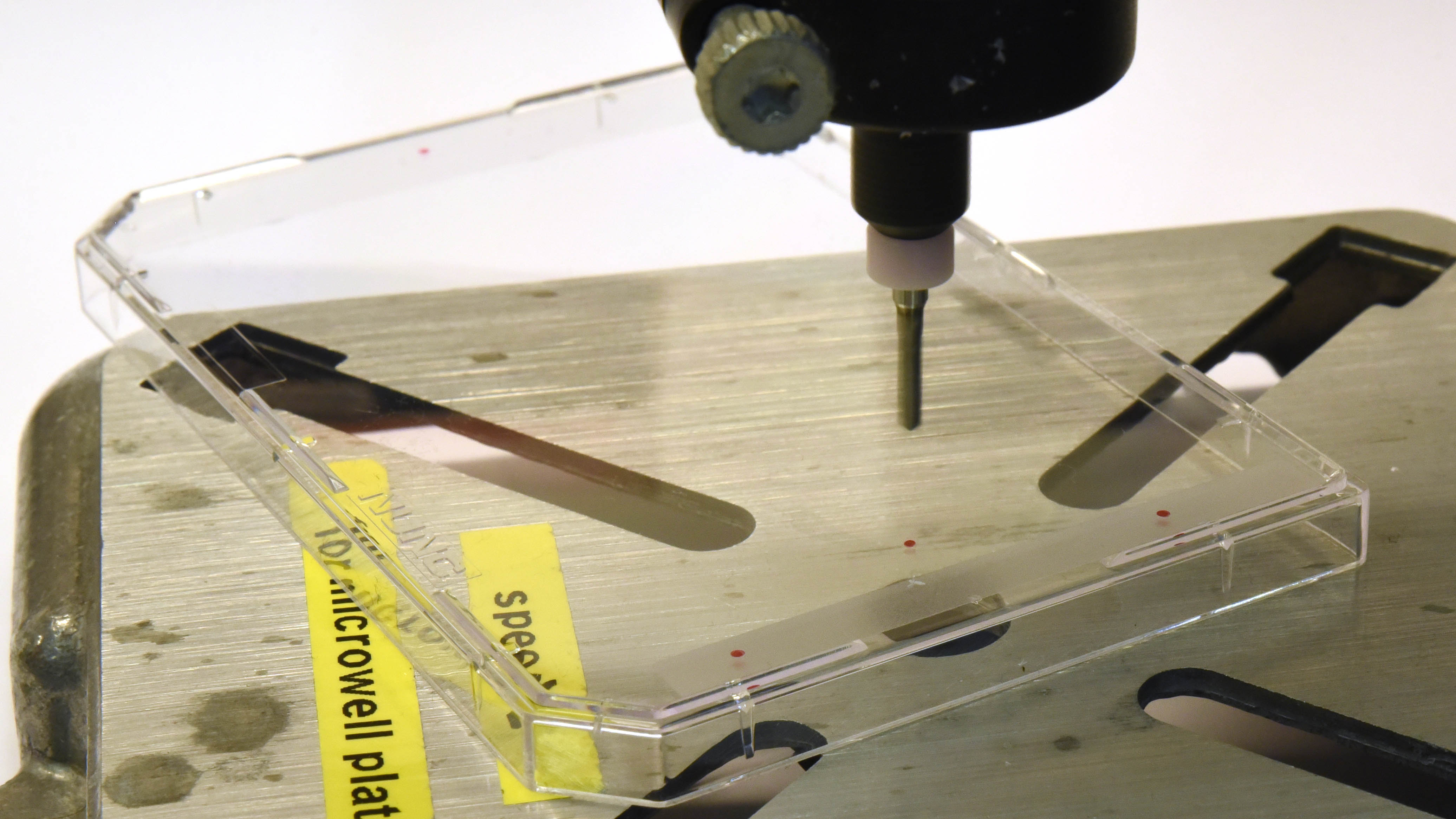
Clean all plastic debris from the lid and wipe with 70% EtOH.
Apply a small amount of cyanoacrylate glue to the bottom of a skimmer nozzle clamp.
Align the clamp with the drilled skimmer hole as below, press firmly, then allow to cure.
Align the drilled hole with the edge of the clamp hole farthest from the slide and bolt. This will prevent pinching if the hole sizes differ significantly.¶
Place the lid on an OmniTray base.
If necessary, trim P200 to length[†].
Insert the inlet and outlet P200 tips firmly into place.
It may be necessary to twist the P200s into final position. With a proper fit, a P200 will sit securely in the drilled hole, with the tip just above the culture surface, but below the expected fluid height (<1 mm, typically).
Note
Small cracks may form around the holes during this step, they can be safely disregarded.
Set the skimmer nozzle height:
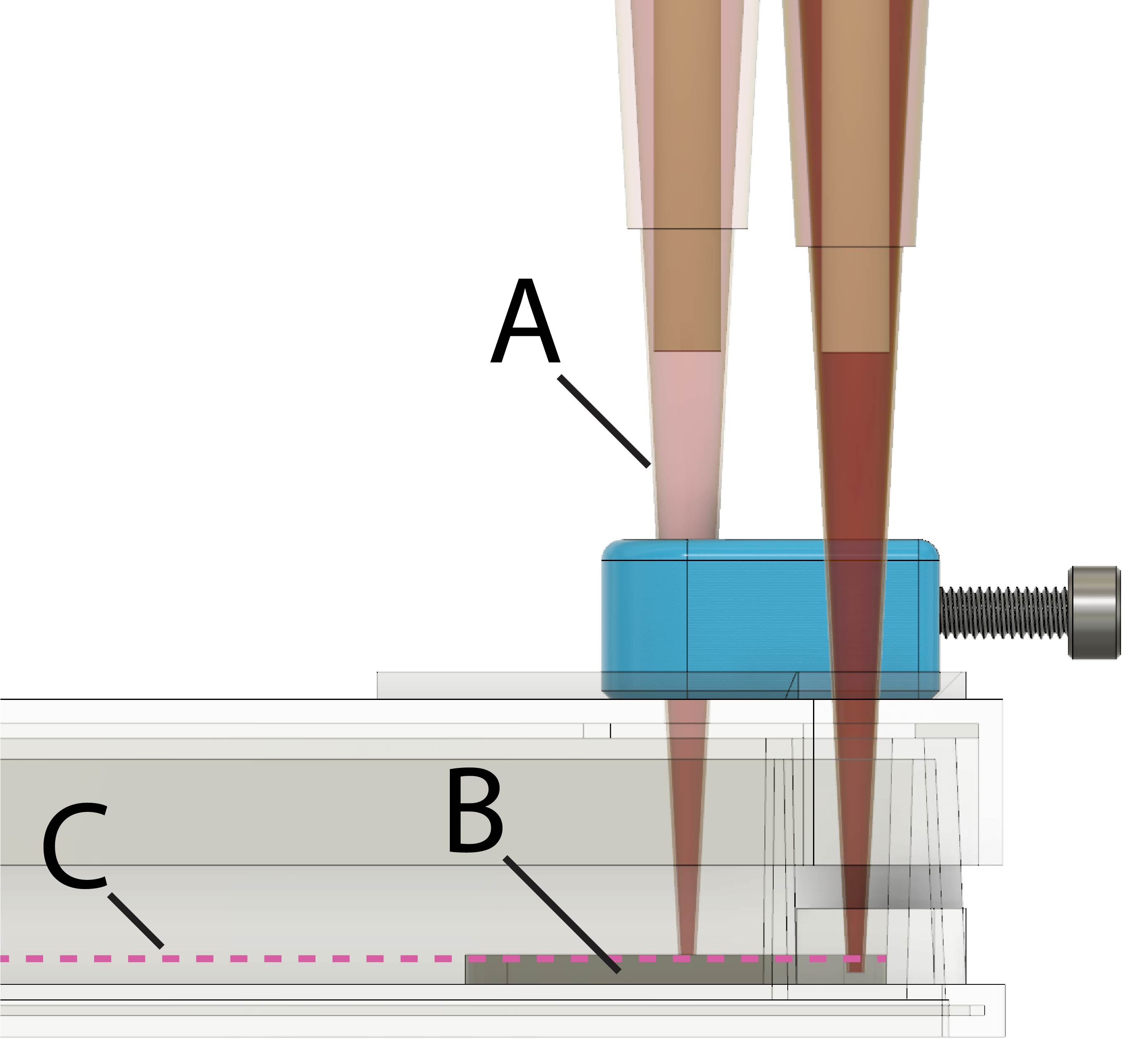
A: Skimmer nozzle P200. B: Skimmer height block. C: Theoretical media level.¶
Insert a P200 into the nozzle clamp.
Select the appropriate
skimmer_height_blockthickness for the desired plate volume. See Selecting Skimmer Height for more.Place the height block in the plate base, underneath the skimmer nozzle.
Note
Keep a spare OmniTray base handy and reuse it for this step, as it’s not advisable to use it for cell culture after this.
Ensure the P200 tip touches the height block and the plate lid sits flat on the base when no force is applied to the skimmer P200, as in the figure above.
While holding the P200 in position, tighten the nozzle clamp bolt using a 2.5 mm hex wrench until the P200 barrel deforms slightly.
Verify the skimmer nozzle position has not changed during clamp tightening
Cut two segments of tubing, 6cm in length, join one end with a Y-piece fitting.
Press fit the open ends of the tubing into the outlet nozzles.
Cut a ~2cm segment of tubing, place it over the remaining Y-piece barb.
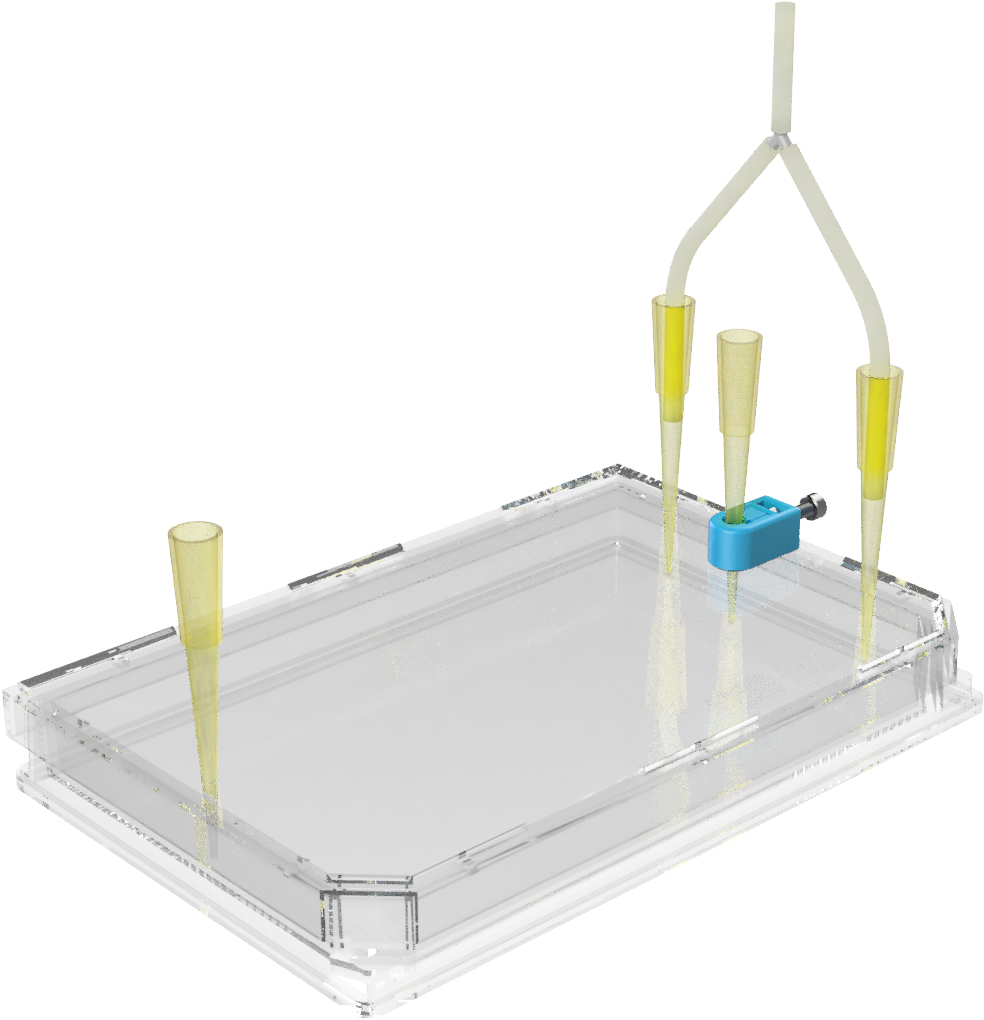
Outlet tubing assembled.¶
UV-sterilize the plate lid prior to use. This can be done, for example, with a standard tissue culture cabinet UV cycle by placing the lid(s) bottom-side-up as close to the UV lamp as possible.
Petri Dish Perfusion Lid¶
6, 10, and 15 cm petri dishes are likely a viable alternative to the rectangular OmniTray, having poorer overall flow characteristics but better availability and variety of size. See the Discussion section in the text, as well as Supplementary Figure 3 for details.
Select the appropriate lid marking jig for the desired petri dish size:
petri_drill_jig_<size>_inlet and petri_drill_jig_<size>_outlet.
Petri dish marking jigs consist of two parts that slide into one another after printing. This provides some adjustment range to accomodate dimensional variabiation between manufacturers.
Assemble the printed jig.
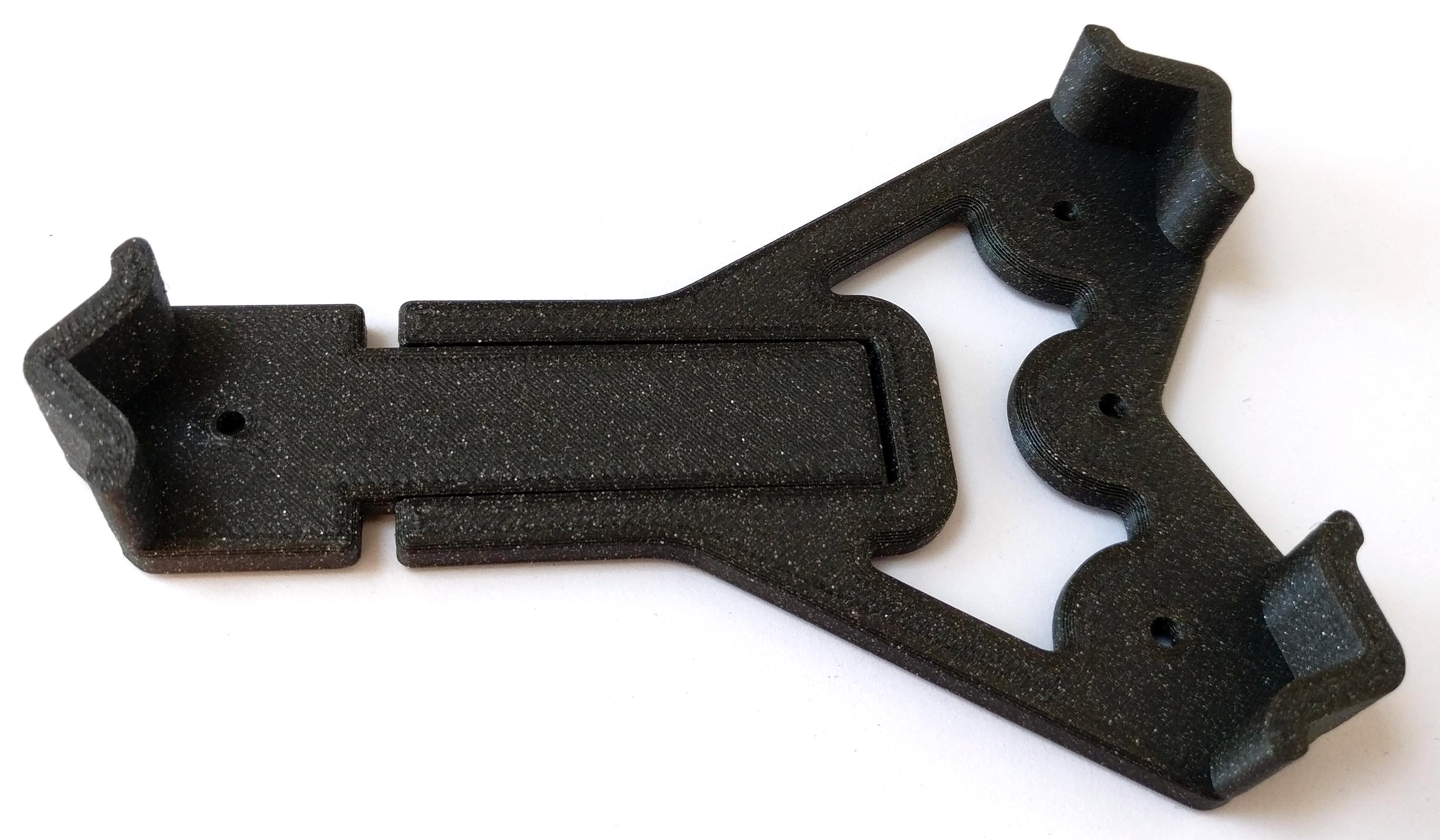
Assembled 10 cm petri lid marking jig.¶
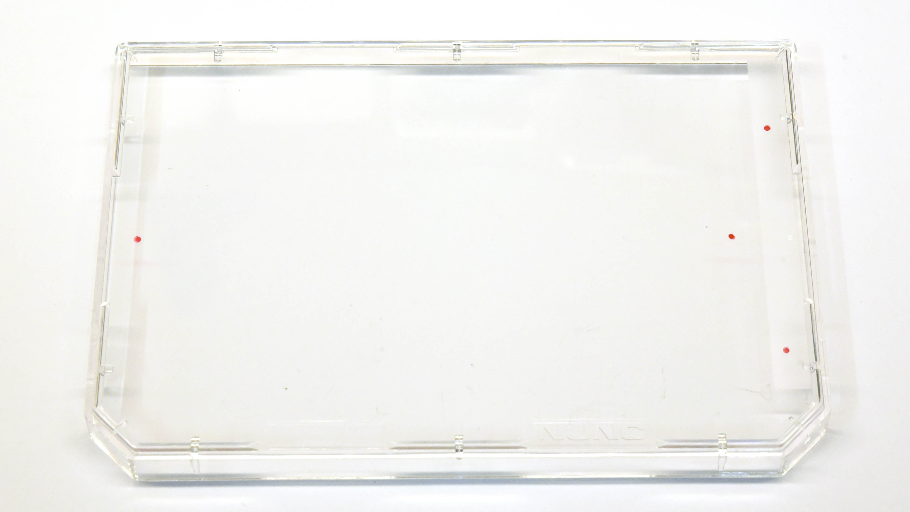
Place the jig atop the plate lid, and while gently holding the two halves together for proper alignment, transfer all four hole locations with a marker.
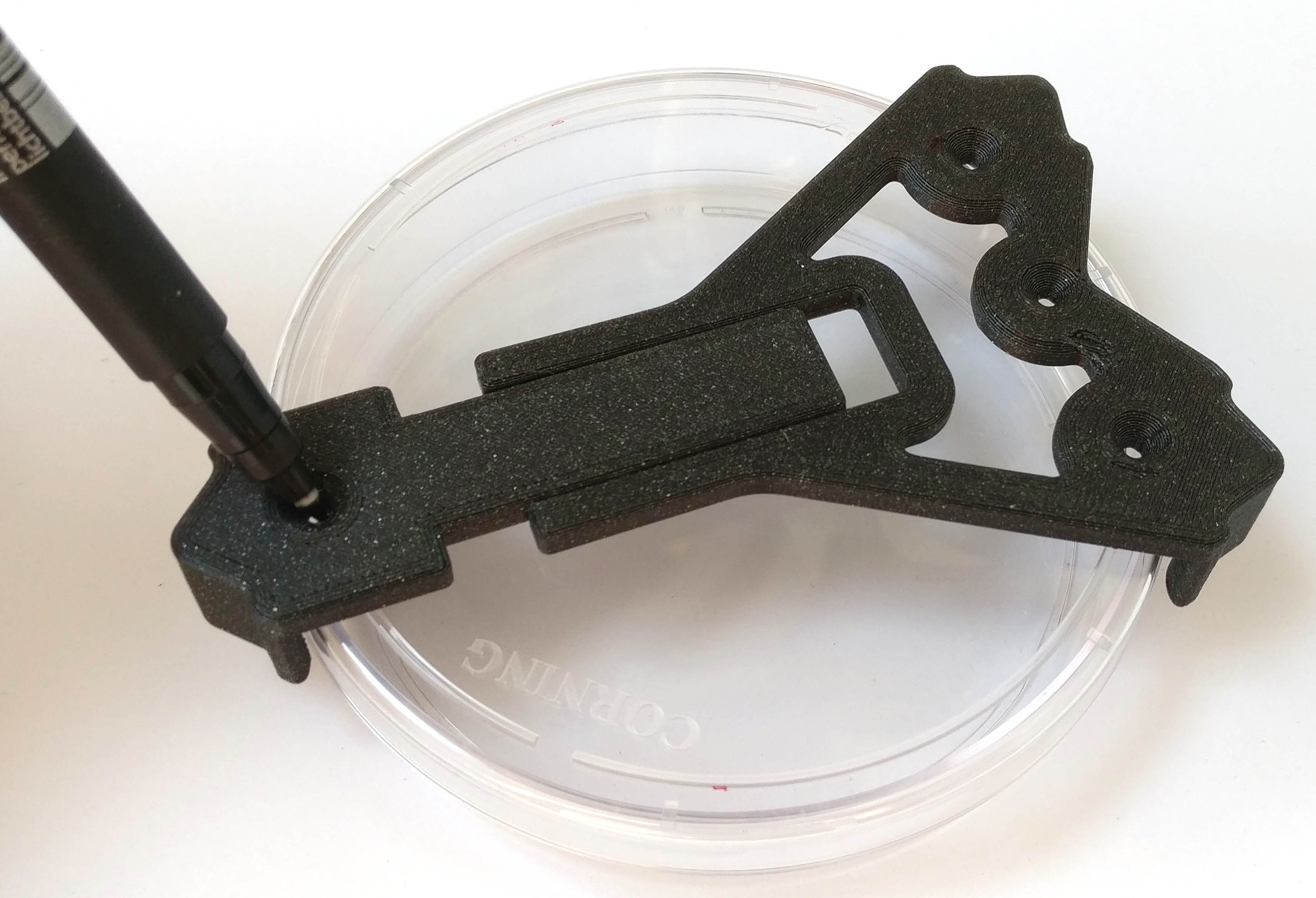
Transferring hole locations to a 10 cm petri lid.¶
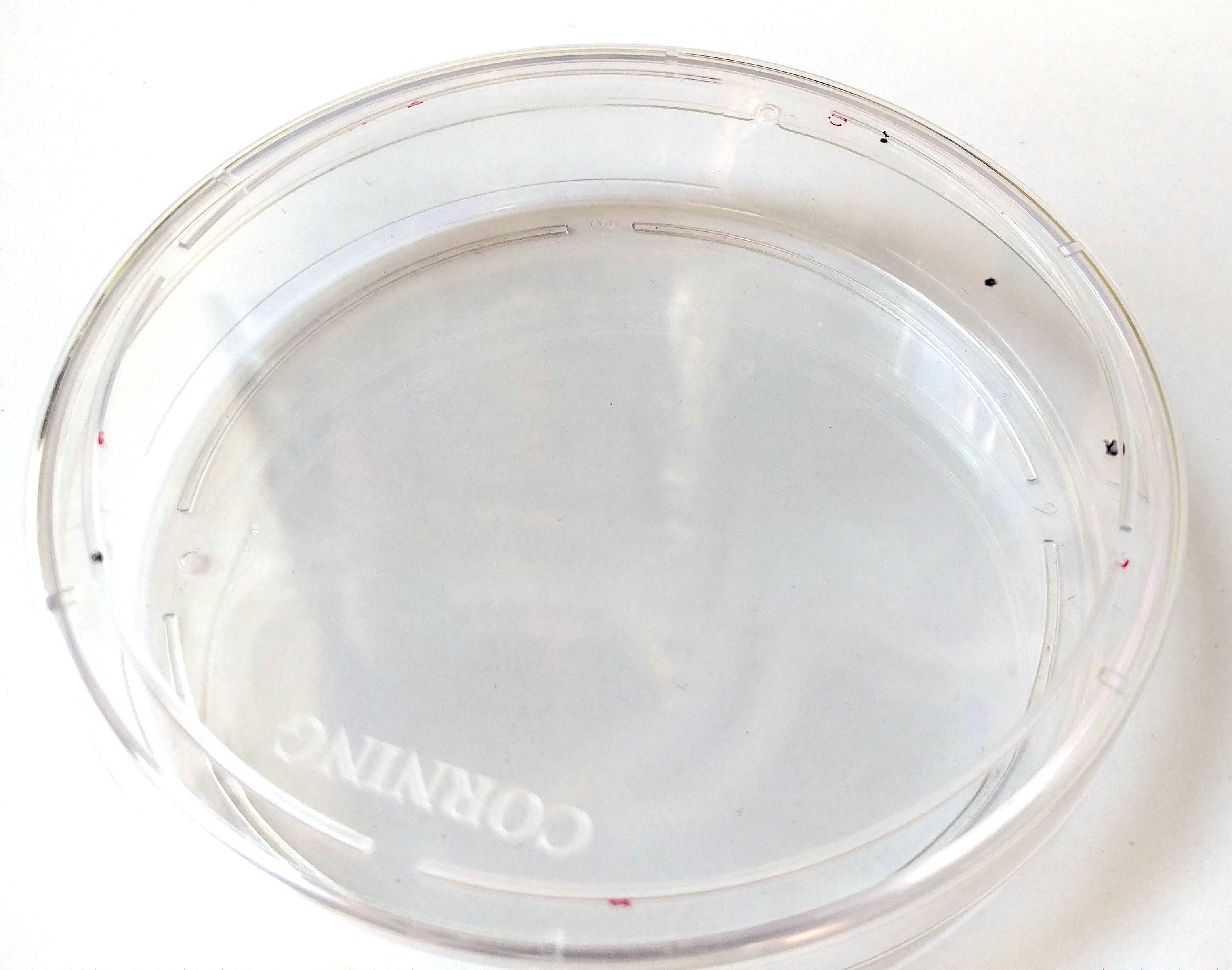
All four nozzle hole locations marked in black ink.¶
With the hole locations marked, remove the lid from the dish and carry on with the build instructions from step 2 in Perfusion Plate Lid above.
Important
As petri dishes are generally deeper/taller than the OmniTray, larger diameter holes will likely be necessary to fully insert the nozzles.
Similarly, the skimmer nozzle height will need to be set higher than in the OmniTray to achieve an equivalent media volume.
References